
GENESIS - Driving sustainable semiconductor innovation in Europe
Project objective
GENESIS (GENerate in Europe a Sustainable Industry for Semiconductor) is a research and innovation project that is co-funded by the European Union. Its objective is to eliminate PFAS chemicals from semiconductor manufacturing through sustainable materials, advanced process monitoring and circular economy practices.
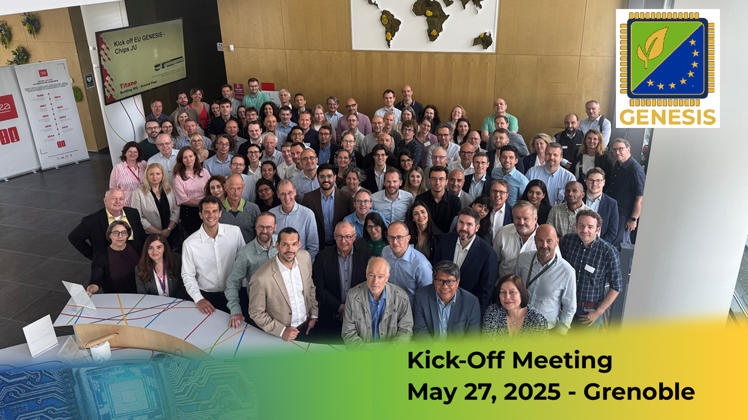
The project was launched in May 2025 and will last for 36 months.
58 partners
GENESIS is a three-year collaborative project coordinated by CEA-Leti, and brings together 58 partners across the European semiconductor value chain. The consortium includes large enterprises, SMEs, research institutes, universities, and industry associations.
LayerOne’s contribution
LayerOne participates in the project as a graphene manufacturer, contributing to the development of new materials with the objective of reducing reliance on critical substances such as PFAS.
The company’s contribution focuses on graphene-based materials and their potential relevance in this context. Graphene is considered both as a possible alternative to PFAS-based materials and as a material of interest for the purification of water containing PFAS.
Four strategic pillars
The project is structured around the development of approximately 45 sustainability-oriented innovations addressing different stages of the semiconductor lifecycle. These activities are organised under four strategic pillars that define the technological scope of GENESIS.
Pillar 1 – Monitoring and sensing focuses on real-time emissions monitoring, traceability, and process feedback systems.
Pillar 2 – New materials addresses the development of PFAS-free chemistries and low-global-warming-potential alternatives for advanced semiconductor processes.
Pillar 3 – Waste minimisation targets improved approaches to recycling, including solvents, gases, and slurries, as well as reuse and the introduction of more sustainable replacements.
Pillar 4 – Critical raw materials mitigation concentrates on reducing dependency on critical raw materials and strengthening resource security.
Complementing these pillars, the project objectives provide an overarching framework that includes the deployment of sensor-integrated abatement systems aimed at reducing PFAS and greenhouse gas emissions. The project also supports the alignment of semiconductor supply-chain practices with environmental regulations, contributing to Europe’s capacity for sustainable semiconductor innovation.